
Insights
SPAD Sensors Reach Volume: Specifying Infrared Detection in 2026
INDUSTRY NEWS · INFRARED & SINGLE-PHOTON DETECTION · SEPTEMBER 2026
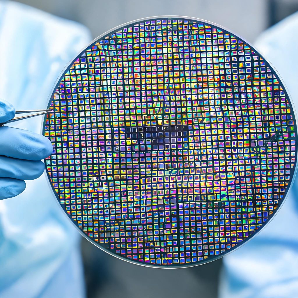
Single-photon avalanche diodes spent two decades as laboratory instruments. In September 2026 two separate publications made the same point from different angles: the technology has moved into the volume tier, and the way buyers should specify infrared detectors is changing with it.
On 26 September 2026, MEMS Consulting published a technology landscape for single-photon avalanche diodes (SPADs). The analysis divides the field into three phases: fundamental p-n junction research before 2008, a CMOS integration phase from 2008 to 2019, and the current optimisation and scaling phase, distinguished by pixel pitches below 4 micrometres and integration at advanced process nodes.
Three drivers are named for the shift from specialist instrumentation to high-volume commercial products: sub-4µm pixel pitch, 28nm CMOS integration, and 3D-stacked sensor-and-logic architectures. Together they allow detection and processing to sit on the same stack rather than in separate chips connected by a board.
An earlier report, on 13 September 2026, showed where that leads at product level. Singular Photonics released Litavis, described as the first SPAD image sensor with in-pixel processing, integrating imaging, timing, histogram generation and photon counting on a single die with on-chip programmable multi-mode operation. A companion paper in the same period described a cryogenic dielectric metalens integrated with a superconducting single-photon detector at 1550 nm, using a smaller active area to reach higher system detection efficiency and adding polarisation-resolved detection.
Why this belongs on an infrared sourcing desk
Short-wave infrared and single-photon detection share a defining property: the signal is faint, so the detector’s noise floor matters as much as its sensitivity. The traditional way to compensate was to enlarge the active area — but as the 1550 nm work notes, a larger area trades away count rate, dark counts and timing jitter. That is the trade-off the new generation of devices is designed to break.
For buyers, that changes what a datasheet conversation should cover. A single headline detection-efficiency figure is no longer sufficient evidence that a part will work in a system.
Explore Infrared Lenses & Optics →
What to put in an infrared detector or module specification
- Dark count rate, not just detection efficiency. In photon-starved applications the noise floor sets the usable range. Ask for dark counts at the operating temperature and bias the design actually runs at.
- Timing jitter when the application involves ranging or coincidence. For lidar, time-of-flight and quantum-adjacent work, jitter determines resolution in a way sensitivity cannot compensate for.
- Pixel pitch and fill factor together. A small pitch is only an advantage if the fill factor and microlens design preserve collection efficiency. Request both numbers.
- Whether processing is on-chip or off-chip. In-pixel processing changes board design, latency and the cost of everything downstream. Treat it as an architecture decision, not a feature.
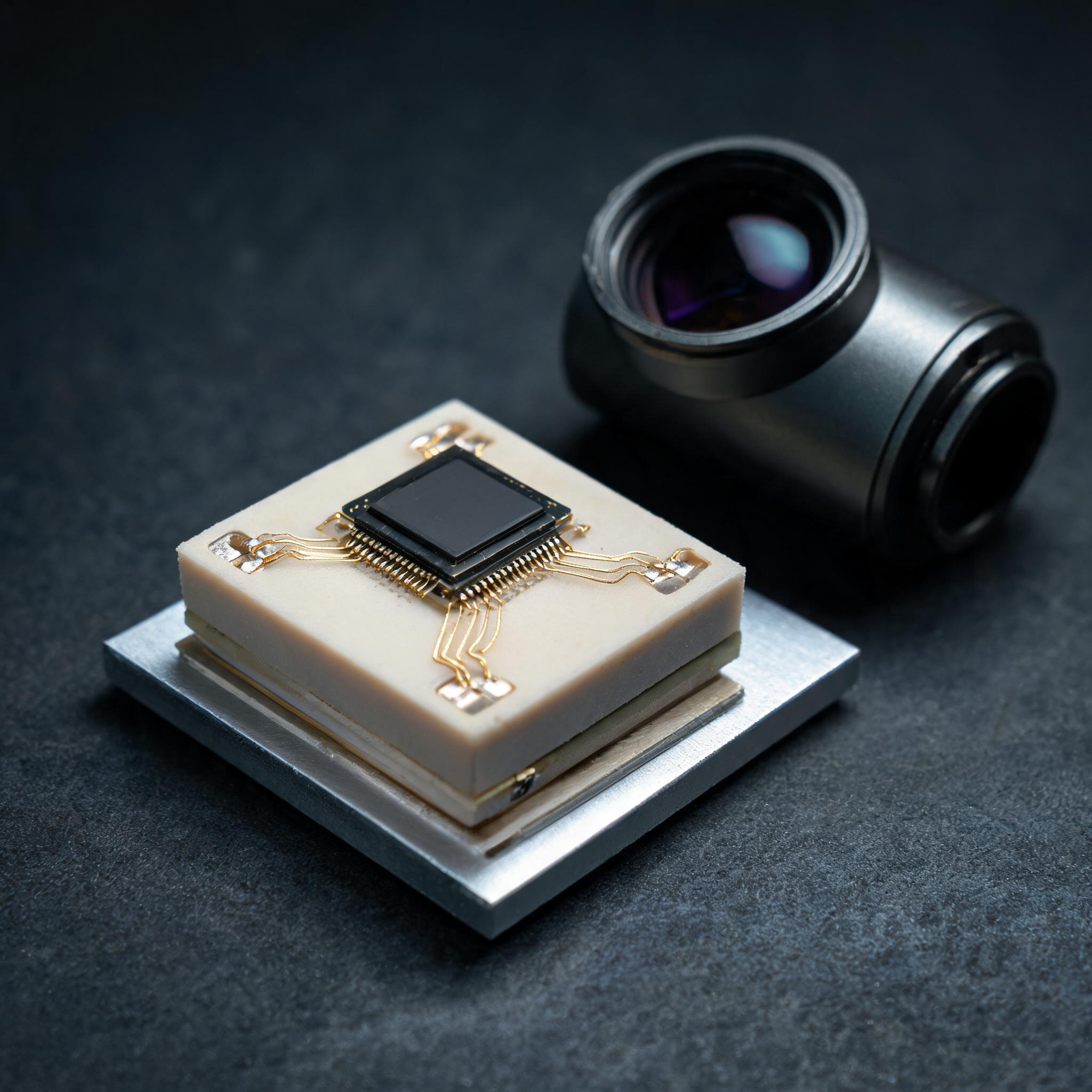
- Optical path and coating as one item. Infrared lenses, filters and windows must be specified with their coatings. A detector specified without its optical path can hit target performance on the bench and miss it in the housing.
- Operating temperature and cooling method. Whether the part is cooled, and how, determines power budget, package size and lifetime. It is a system decision that is expensive to revisit.
Sourcing observations
- Separate visible-light and infrared quotations by default. Materials, coating stacks and inspection methods differ enough that a combined quotation hides where the cost actually sits.
- Qualify with distribution data, not typical values. Infrared detector performance varies with process and temperature. Ask for measured distributions across a production lot.
- Test in the final housing. Assembly stress and stray light routinely degrade performance relative to bare-chip measurements. First-article approval should be at module level.
- Expect the unit of purchase to move up. As detectors gain on-chip processing, buying a characterised module instead of a bare sensor reduces integration risk for most buyers.
- Watch the pixel-level trend when planning tooling. If processing continues to migrate into the pixel, future module designs will have fewer components, not more. Avoid tooling that assumes today’s component count is permanent.
Sourcing infrared lenses, windows or detector modules?
Send your wavelength range, aperture and focal length, coating requirements, annual volume and delivery window to sales@tuolango.com and we will return a sourced comparison including coating options and lead times.
Sources and disclosure
Sources: MEMS Consulting (mems.me) SPAD technology landscape published 26 September 2026 covering patent and literature trends, the three-phase development model, sub-4µm pixel pitch, 28nm CMOS integration and 3D-stacked architectures; MEMS Consulting report of 13 September 2026 on Singular Photonics’ Litavis SPAD image sensor with in-pixel processing; and MEMS Consulting report of 13 September 2026 on a cryogenic dielectric metalens integrated with a superconducting single-photon detector at 1550 nm for higher system detection efficiency and polarisation-resolved detection. The specification, sourcing and procurement observations above are TUOLAN TRADE analysis and are not attributed to any cited source. Edited and analysed by TUOLAN TRADE.