
Insights
Silicon Carbide Waveguides Move From Option to Production: AR Optics Sourcing
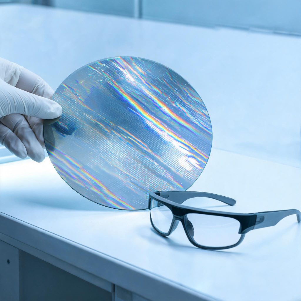
PRECISION OPTICS · AR WAVEGUIDES & SUBSTRATES · SEPTEMBER 2026
Silicon carbide has spent three years as the AR waveguide material that could deliver 70° field of view if only someone could make it in volume. In 2026 that stopped being a materials question. Substrate, chip and module lines are all adding capacity at the same time — and cost, yield and supply chain maturity are now the three gates that decide the timeline.
The starting point was a demonstration, not a product. In 2024 Meta’s Orion prototype used a silicon carbide waveguide to reach a 70° field of view, which showed what the material could do. Making 70° on a bench and shipping 70° at a workable price are two different problems, and 2026 is the year the industry started addressing the second one.
Why SiC keeps winning the physics argument
Three material properties explain the interest, and they compound:
- Refractive index around 2.6–2.7, against roughly 1.9–2.0 for conventional optical glass and about 1.74 for resin. A higher index delivers a larger optical étendue and a wider K-domain, so a single-layer waveguide can support a 50°–70° field of view, where glass stacks typically need multiple layers to reach about 40°. Goertek’s F50Se module is cited as using SiC to break past the roughly 30° limit of a glass substrate and reach 50° FOV.
- Thermal conductivity around 490 W/mK, roughly two orders of magnitude above ordinary optical glass. Heat from the light engine can leave through the waveguide lens itself, which removes a temple-side thermal module and frees design space in the frame.
- Low dispersion, quoted below 0.03. A higher index compresses the effective wavelength and shortens the grating period, which addresses rainbow artifacts in full-colour display at the source rather than in software.
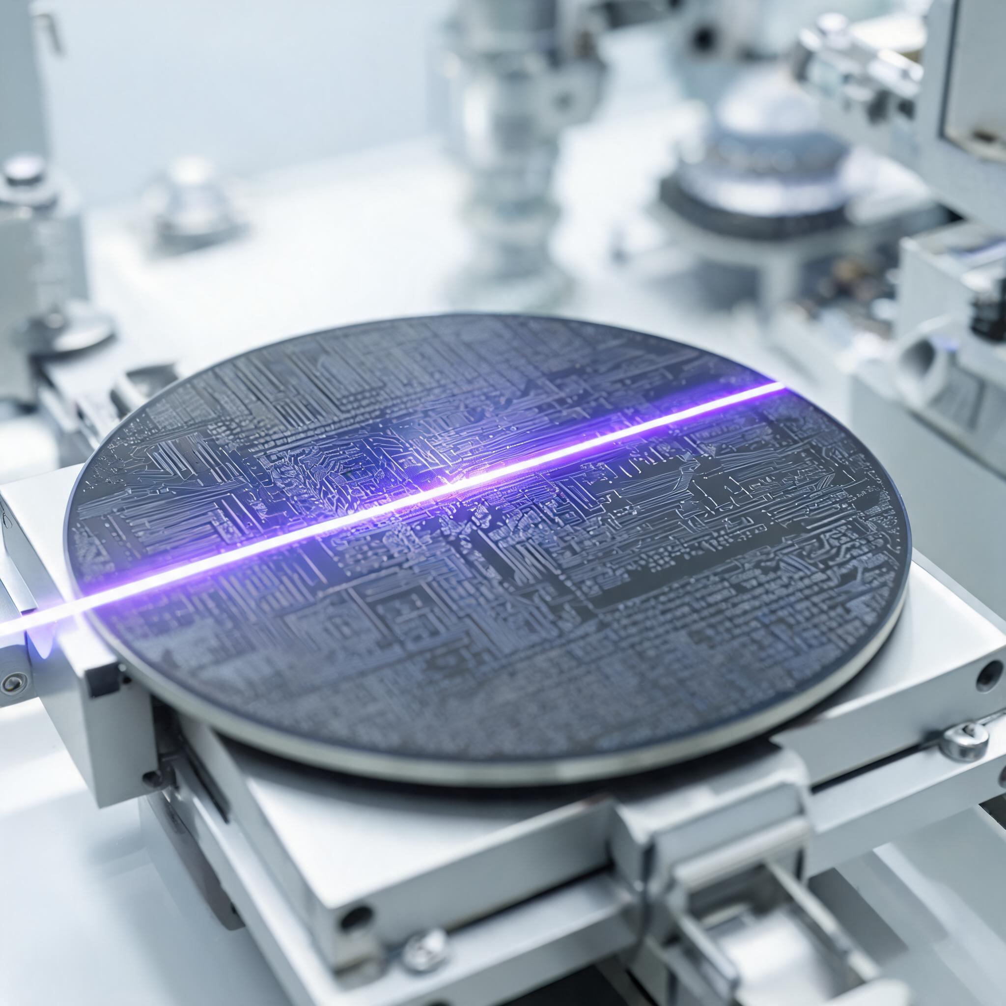
Three lines moving at once in 2026
What changed this year is that the three parts of the chain started scaling together, rather than one at a time:
- Substrate. Tianyue Advanced (SICC) has released a full 12-inch SiC substrate family, and optical-grade AR substrates are extending from the power-electronics substrate base into waveguide lens processing. San’an Optoelectronics’ 6-inch and 8-inch optical wafers are reported to have passed validation with leading international customers and to be shipping in small volume, with 12-inch at sampling stage.
- Chip and wafer. AlphaLens closed an oversubscribed Series B above RMB 100 million to build an 8-inch SiC metasurface waveguide chip line, with RMB 140 million planned for a high-volume metasurface photonic chip centre and a first-phase capacity of 500,000 wafers per year, expandable to the million range at full ramp.
- Module. Guangna Siwei’s SiC full-colour waveguide is quoted below 0.6 mm thick and under 3 g and is already in volume use in the Coray Air2 commercial AR glasses. Goertek’s F50Se module pairs a full-colour LCoS engine to deliver above 1500 nits into the eye.
The manufacturing base is following. Goertek reports that China’s first 12-inch wafer DUV lithography-and-etch volume line has been commissioned, and Guangna Siwei has built a million-set-class fully automated nano-imprint line. SiC processing is moving from laboratory handling toward wafer-level production.
Three gates remain: cost, yield, supply chain
- Cost. The SiC AR waveguide market was around US$5 million in 2025, is expected to reach about US$21 million in 2026, and roughly US$130 million by 2032 — a compound growth rate of about 35.5%. Current SiC waveguide average selling prices sit at US$250–350 per piece, well above glass. An 8-inch SiC wafer yields roughly four lenses; a 12-inch wafer yields roughly ten. Moving to larger substrates is the main lever on price.
- Processing yield. SiC is extremely hard, so dicing, grinding and polishing yield far below glass. Etching needs high-precision electron-beam lithography and reactive ion etching, and industry yield is still climbing.
- Supply chain maturity. The full chain — substrate, lens blank, patterning (e-beam, DUV or nano-imprint), etch or imprint, coating, dicing, bonding, module packaging — is still being built. The 12-inch DUV line is a significant step, but matching glass-method maturity will take time.
What this means if you buy optics
- Treat waveguide optics as a camera-class business, not a niche. The same precision-lens, coating and metrology supply chain that serves visible-light and near-infrared objectives is being pulled into AR waveguide programs. Buyers already qualified in VIS–NIR optics have a shorter path in.
- Specify the substrate grade, not just the material. Optical-grade SiC is a different specification from power-electronics grade. Defect density, surface finish and flatness belong in the drawing.
- Price the whole chain, not the die. Patterning and packaging typically dominate total cost well before the substrate does. Ask for a step-by-step cost breakdown so the improvement lever is visible.
- Do not plan a consumer price point before 2027. The physics is settled and volume is being built, but current per-piece pricing means SiC stays in the premium tier through at least the next product cycle.
- Keep a glass or hybrid fallback qualified. For 25°-class AI-interaction eyewear, glass and nano-imprint routes remain the practical volume choice while SiC capacity matures.
Sourcing precision optics, windows or coatings?
Send your drawing, substrate or material grade, coating specification, annual quantity and target delivery window to sales@tuolango.com and we will return a sourcing comparison with qualified suppliers and lead times.
Sources and disclosure
Sources: OFweek Optics analysis of 28 September 2026 on silicon carbide AR waveguides — refractive index 2.6–2.7 versus 1.9–2.0 for optical glass and 1.74 for resin; single-layer 50°–70° field of view; thermal conductivity around 490 W/mK; dispersion below 0.03; Goertek F50Se 50° FOV module with full-colour LCoS above 1500 nits; Meta Orion’s 70° prototype in 2024; Tianyue Advanced 12-inch SiC substrate family; San’an Optoelectronics 6-inch and 8-inch optical wafers validated and 12-inch at sampling; AlphaLens Series B above RMB 100 million for an 8-inch metasurface waveguide chip line with RMB 140 million investment and 500,000-wafer first-phase capacity; Guangna Siwei SiC full-colour waveguide below 0.6 mm and under 3 g in Coray Air2; China’s first 12-inch wafer DUV lithography-and-etch volume line and a million-set nano-imprint line; market size about US$5 million in 2025, about US$21 million in 2026 and about US$130 million by 2032 at a 35.5% compound growth rate; SiC waveguide pricing of US$250–350 per piece with roughly four lenses per 8-inch wafer and ten per 12-inch wafer. Procurement and qualification observations are TUOLAN TRADE analysis and are not attributed to any cited source. Edited and analysed by TUOLAN TRADE.