
Insights
400G-per-Lane MUTC-PD Sample Points at 3.2T Receivers
INDUSTRY NEWS · FIBRE OPTICS & TRANSCEIVERS · SEPTEMBER 2026
Every 1.6T and 3.2T optical module is limited by two chips: the laser that sends the light and the photodiode that receives it. China has spent three years talking about the first. A 2024-founded startup showed the second at CIOE 2026, and the design detail it published is a better sourcing signal than the press release.
On 20 September 2026, Optical Fiber Online published an interview with Kualin Photonics (快甎光电), a photodetector chip company founded in 2024 and spun out of ShanghaiTech University, where its core team came from the same research group under Professor Chen Baile. The team is described as holding PhDs from that group, with an average age under 30, and the company focuses on high-speed, high-power III-V photodetector chips.
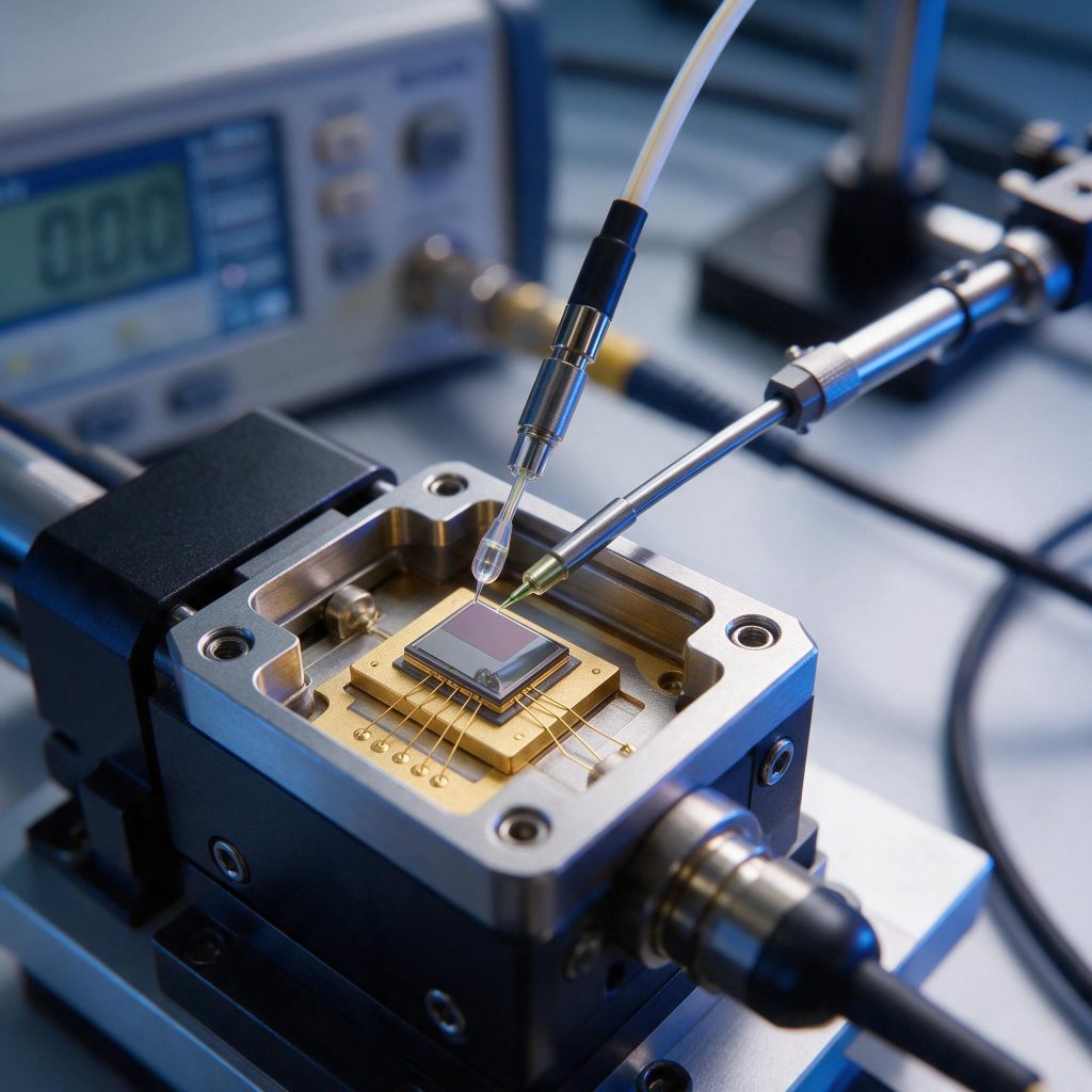
The reported milestones are specific. In June 2026 the company closed an angel round of several tens of millions of RMB. At CIOE 2026 it exhibited a single-lane 400G photodiode sample built on a modified uni-travelling-carrier structure, which the company calls MUTC, and positioned that part for 3.2T optical modules. The sample uses a back-illuminated coupling design with a microlens integrated on the back of the chip.
Why the receiver side is the harder conversation
Optical interconnect has moved to 200G per lane and is now specifying 400G per lane. Transmitter-side coverage in China is comparatively well documented, with multiple 200G-class electro-absorption modulated laser programmes in various stages of qualification. The receive side is less so. High-end photodetector chips have been dominated by overseas suppliers, and the reported domestic pattern has been single-point technical results rather than a full chain from device design through III-V epitaxy and packaging to yield.
- The stated bottleneck is linearity, not raw bandwidth. A conventional PIN photodiode loses performance under high optical input. A standard UTC structure improves speed and power handling but still drifts as optical power changes. The MUTC claim is a wider incident optical power range with stable bandwidth and frequency response, which is the specification a 3.2T link actually punishes.
- Back-side coupling with an integrated microlens is a packaging decision as much as an optical one. It changes the assembly sequence, the alignment tolerance budget and the active-alignment time in the module house. That is a cost question before it is a performance question.
- The funding is early-stage. Tens of millions of RMB is a sample-to-pilot budget, not a volume capacity budget. The stated use is to iterate the high-speed chips and accelerate single-lane 200G and 400G production readiness, and to hire.
- A 2024 vintage company changes your qualification timeline. A supplier that did not exist three years ago will not have a multi-year field-return record. Buyers who require one should plan for that gap rather than assume comparable data will appear.
Explore our Optical Transceivers →
What an optics buyer should actually do with this
- Ask for a linearity curve, not a bandwidth figure. Request responsivity, dark current and frequency response plotted against incident optical power at your operating wavelength and temperature. A part that is fast at low power and drifts at high power will fail in a 3.2T link.
- Qualify the coupling route before the die. If your module design assumes top-illuminated active alignment, a back-illuminated part with an integrated microlens may not drop into your existing process. Confirm the intended coupling scheme and the alignment tolerance the supplier expects to meet.
- Separate sample availability from delivery capability. A CIOE sample and a predictable monthly delivery schedule are different commitments. Ask for the wafer start cadence behind the samples.
- Keep a second source qualified in parallel. Early-stage domestic receiver chips are a strategic hedge against imported parts, not yet a replacement for a qualified incumbent. Run both through your reliability plan rather than switching on price.
- Check the III-V epitaxy route. The chain from device structure to epitaxy to packaging yield is where domestic photodetector programmes historically stop. Ask whether epitaxy is in-house or foundry-supplied, and whether that source scales with you.

Sourcing 400G-per-lane receivers, photodiodes or complete transceivers?
Send your lane rate, wavelength, reach, coupling scheme and annual volume to sales@tuolango.com and we will return a supplier comparison with sample and pilot-run options.
Sources and disclosure
Sources: Optical Fiber Online (c-fol.net) interview with Kualin Photonics published 20 September 2026, covering the company’s founding year, its origin from a ShanghaiTech University research group, the June 2026 angel round of several tens of millions of RMB, the single-lane 400G MUTC photodiode sample shown at CIOE 2026, its back-illuminated coupling design with an integrated back-side microlens, the intended 3.2T module application, and the company’s statement that high-end photodetector chips have been dominated by overseas suppliers. All figures and technical descriptions are reproduced as the cited source states them; the company’s performance claims about the MUTC structure have not been independently verified by us and no measured data was published in the source. Details of customers, delivered volumes, qualification status and pricing were not disclosed and are not estimated here. This article is original editorial analysis by TUOLAN TRADE for industry reference, not investment advice or an offer of securities. Product and company names remain the property of their respective owners.